nRF52 Debug Resurrection (APPROTECT Bypass) Part 1
**Yes, resurrection of JTAG/SWD interface on protected platforms has always been a sensitive topic in embedded security**....
Yes, resurrection of JTAG/SWD interface on protected platforms has always been a sensitive topic in embedded security.
This security investigation presents a way to bypass the APPROTECT on a protected nRF52840, in order to reactivate the Serial Wire Debug Interface (SWD), offering full debug capabilities on the target (R/W access to Flash/RAM/Registers, Code Exec and reprogramming). All the nRF52 versions are impacted.
Due to its intrinsic characteristics, the vulnerability cannot be patched without Silicon redesign, leading to a countless number of vulnerable devices on the field forever.
Nordic Semiconductor and LimitedResults did not agree on a responsible disclosure.
1. About nRF52 Series SoC Family
The entire nRF52 family consists of six different nRF52 platforms, all built around the ARM Cortex-M4F CPU.
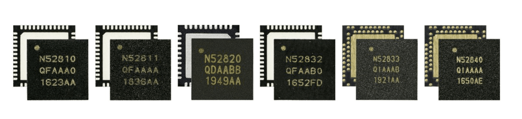
The entire Nordic nRF52 Series SoC Family
A comparison table between the different platforms is available here.
Let's focus on the family flagship, the nRF52840.
2. The Target: nRF52840
The nRF52840 System-on-Chip (SoC) is the most advanced member of the nRF52 Series SoC family. It is an advanced Bluetooth, Thread and Zigbee multi-protocol SoC built around a 64 MHz Cortex-M4F CPU. It comes with 1MB of Flash and 256Kb of RAM, both fully integrated.
In term of security, the ARM TrustZone CryptoCell cryptographic unit is integrated as cryptographic engine. The block diagram gives an idea of the capabilities (and the complexity) of the nRF52840:
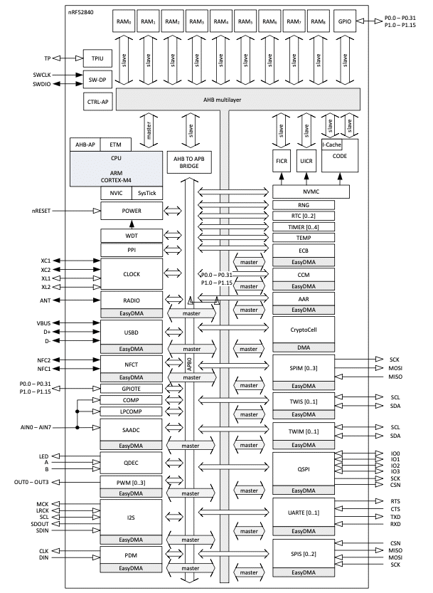
Block diagram of the Nordic nRF52840
3. Code Readout Protection
Nowadays, most of the Semiconductor Vendors implement a security feature called Code Readout Protection inside their MCUs/SoCs, preventing an attacker with physical access to dump the Code/Data stored in the integrated Flash Memory and also to modify it.
This security feature can have different names depending on the chip vendors (CRP, RDP, PCROP...)
Generally, once an attacker has a copy of the Firmware, he can start the reverse engineering process or just grab some sensitive data (such as keys and passwords).
3.1 Previously on the nRF51 serie**s
Back in 2015, Include Security found a vulnerability in the design of the nRF51 code readout protection feature (called RBPCONF), allowing an attacker to recover the entire Firmware using the SWD debug interface.
On the nRF51, once the RBPCONF protection is enabled, using the debugger to access directly the Flash or RAM return nothing but zeros. However, it is still possible to control the code execution and read and write to registers (even to Program Counter). So finding a “gadget” in the protected memory such as a simple load word instruction that read memory from an address in some register to another register is sufficient to extract the entire Firmware. Consequently, an attacker with physical access to an nRF51-based device, is able to dump the Flash, exploiting this design vulnerability.
Thereby, nRF51 code readout protection (RBPCONF) is considered as a broken security mechanism and does not protect against Firmware Extraction.
3.2 Access Port Protection APPROTECT on nRF52
After this fail, NordicSemiconductor decided to design the nRF52 with a more restricted security mechanism in order to protect against Memory Readout. This security feature is called Access Port Protection (APPROTECT), mentioned very briefly in the nRF52 Datasheet:
nRF52 Overview
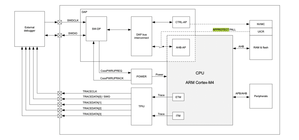
Typically, an external debugger is accessing the ARM CPU through the Debug Access Port (DAP). Then, two different ports are available:
- CTRL-AP. This is the Master Debug Port and it is not dependent of APPROTECT. It will be used to recover, in case of bricked device for example.
- AHB-AP. This the real Debug Port to access memories and control the CPU via SWD.
NordicSemiconductor does not provide any information about the APPROTECT mechanism. I recommend to read ARM reference documentation of Cortex-M.
3.3 UICR
User Information Configuration Registers (UICR) are non-volatile memory (NVM) registers for configuring user-specific settings. They are mapped at 0x10001000.
APPROTECT belongs to UICR. It is necessary to write 0xFFFFFF00 at address 0x10001208 to enable the Access Port Protection, as shown below:
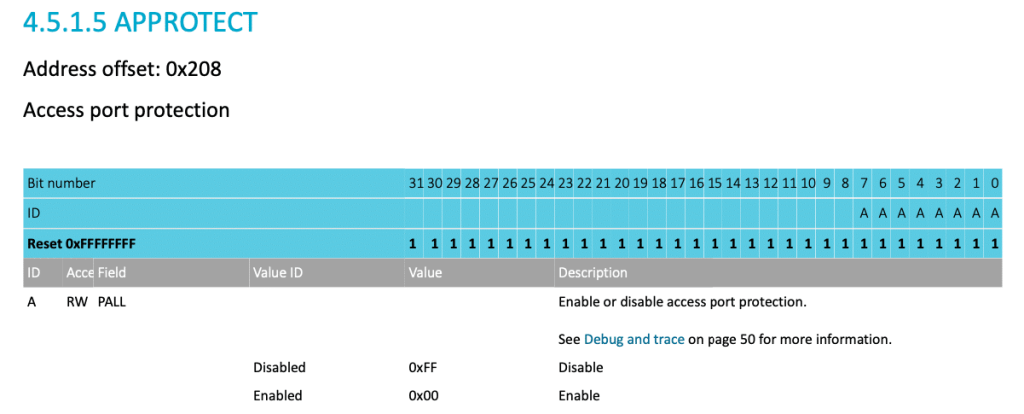
APPROTECT Configuration Register
Power-on-Reset is then required to apply new settings present in UICR.
According to Nordic, the APPROTECT security cannot be disabled without erasing all the RAM and Memory Flash.
4. Setting the environment
4.1 nRF52840 Dev-Kit
The development Kit nRF52840-DK is used for the tests, based on nRF52840.
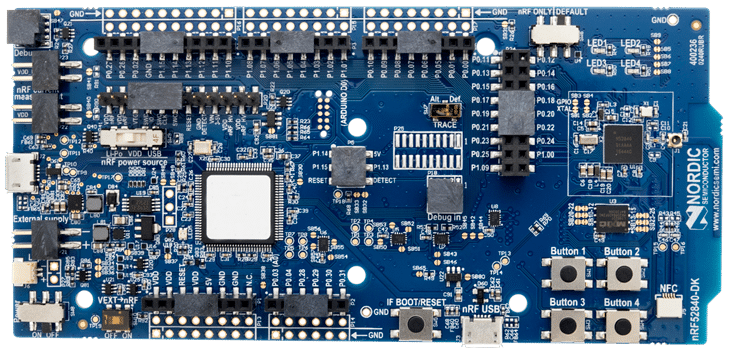
nRF52840 Dev-Kit. The target is the little chip on the right.
The User Manual and schematics are available on the manufacturer’s website. The nRF52840 is a QFN73 version, 7x7mm, located on the right.
This kit has an embedded Segger J-Link debugger (the biggest chip with a white sticker).
The SDK is the latest version available now nRF5_SDK_16.0.0_98a08e2.
Nrfjprog v10.6.0 and JLink v6.64 are used as command line tools.
As a quick start, I just compile and flash an example from the SDK to check my environment is OK. Everything runs smoothly, I can focus on the APPROTECT security feature.
4.2 Enabling the APPROTECT
Method 1 (via OpenOCD):
$ openocd -s /usr/local/share/openocd/scripts -f ./interface/jlink.cfg -c "transport select swd" -f ./target/nrf52.cfg
#Telnet
$ telnet localhost 4444
> flash fillw 0x10001208 0xFFFFFF00 0x01
> reset
Method 2 (via nrfjprog):
$ nrfjprog --memwr 0x10001208 -- val 0xFFFFFF00
After that, any attempt to connect the CPU will fail, displaying “Error: Could not find MEM- AP to control the core”:
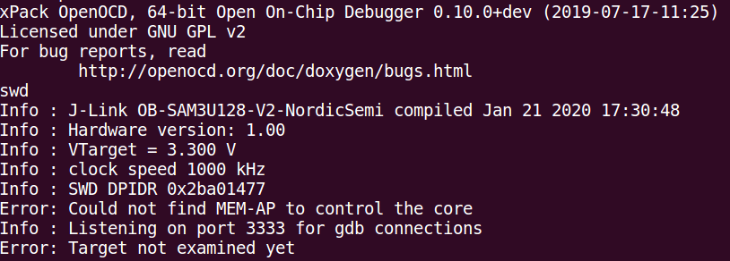
SWD is disabled, due to the activation of the APPROTECT.
Any attempt to attach GDB displays the error:
Error: attempted 'gdb' connection rejected
4.3 Disabling the APPROTECT
Method 1 (via OpenOCD):
# Read APPROTECTSTATUS
# (0x0 Access port protection enabled - 0x1 APP disabled)
> nrf52.dap apreg 1 0x0c 0x00000000
# Write ERASEALL register
> nrf52.dap apreg 1 0x04 0x01
> reset
Method 2 (via nrfjprog):
$ nrfjprog -f NRF52 --recover
All Flash and RAM are erased during the process. After a Reset, the nRF52 can be programmed again.
5. Attack Strategy
5.1 Boot Process
The Boot Process is relatively simple, due to the fact that the nRF52840 does not contain bootROM code (so no embedded boot-loader routines, nor IAP/ISP routines to reverse-engineer…)
The entry point is 0x000002B4, located in Flash memory:
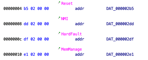
I used Ghidra...economic times are tough.
So far, it is really simple. All the blocks, like the NVMC, the memories, the Debug Acces Port… are initialised purely in Hardware.
5.2 Reset
Several sources may trigger a reset. All the reset sources and their targets are summarised in the table below:
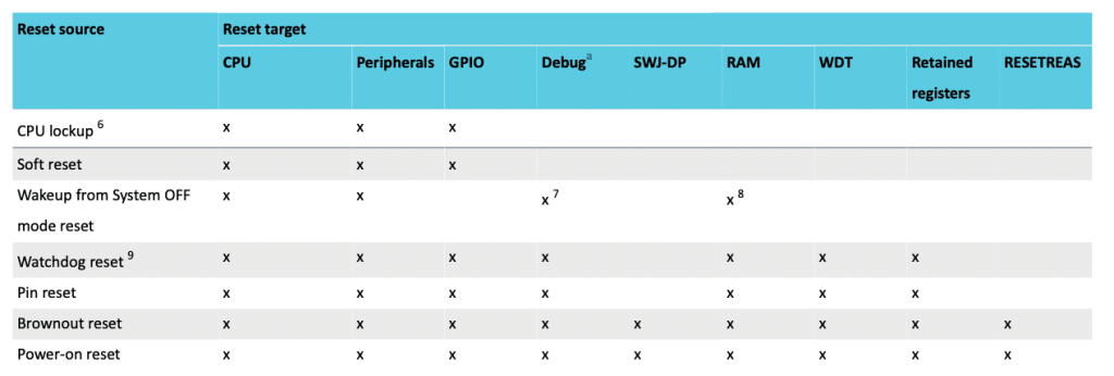
Reset Table
The last line is interesting. A Power-on Reset will reset the entire SoC, included the Debug Port.
5.3 The Limited Plan
The goal is to re-enable the access to the AHB-AP Debug, despite of the APPROTECT.
After a Power-on Reset, the AHB-AP has to initialise itself according to the value of the APPROTECT, which is stored in UICR (a dedicated Flash memory partition).
During the boot, the Memory Controller (NVMC) has to communicate with the CPU (or with the AHB-AP Block directly) to provide the APPROTECT value stored in Flash, and then set its protection state accordingly.
Due to the absence of BootROM, this is achieved by pure Hardware and it has to be done during the early boot process, before the CPU start to load from Flash and execute Code.
My goal is to identify this “pure HW process” and then try to modify the AHB-AP Debug Initialisation. If successful, the Debug features will be reactivated until the next Power-on Reset.
Fault injection is (again) the only way to go here.
6. Target Preparation
6.1 Power Configuration
The system contains two different regulator stages, REG0 and REG1. Each regulator stage has two different and configurable options based on Low-dropout Regulators (LDO) and Buck Regulators (DC/DC).
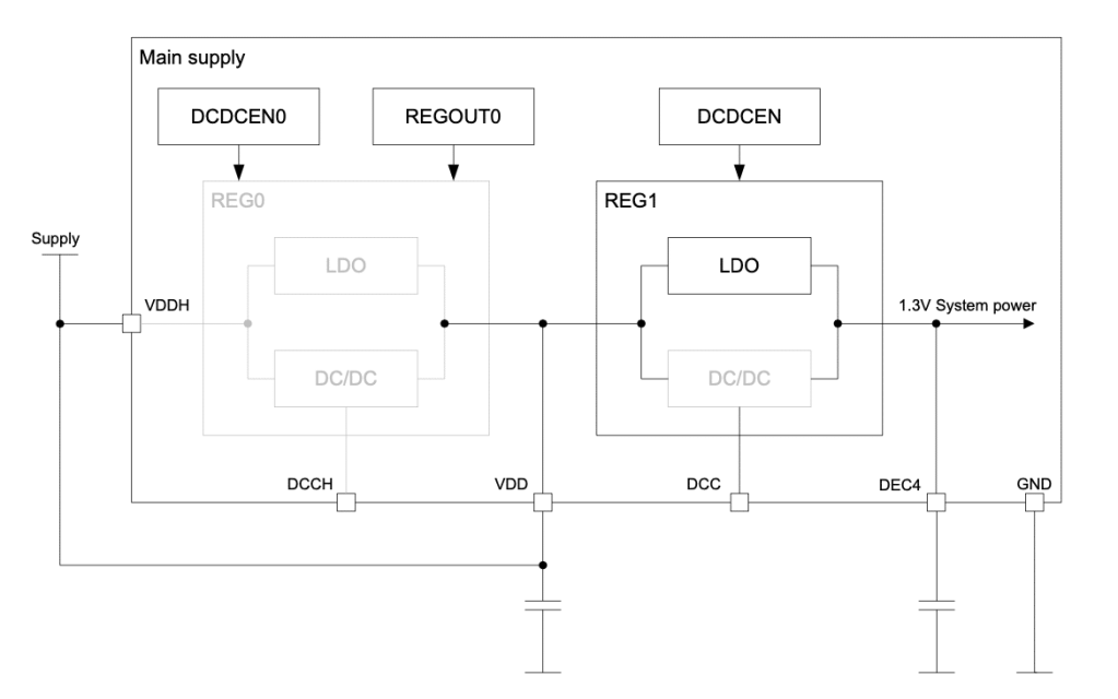
Normal Voltage mode on nRF52840, with only LDO enabled
Only DEC4 is mentioned on the schematic above.
I am particularly interested by the DEC pins (DEC1, DEC2 until DEC6), where external decoupling capacitors are connected. NordicSemiconductor does not provide any detail about the nRF52 power network.
After a quick probing session, I decide to focus on DEC4 (1.2V-1.3V) and DEC1 (0.8V-0.9V):
-
DEC4 is the power line after the REG1 stage. So it probably supplies the entire digital system (CPU & memories)
-
DEC1 is definitively the CPU power line.
6.2 PCB Modification
To analyse the activity inside the chip, it is necessary to slightly modify the PCB:
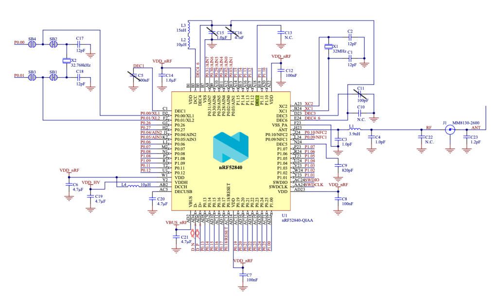
PCB Schematic. Some capacitors has been removed.
The corresponding decoupling capacitors C5, C15, C16 and C11 are removed.
6.3 Fault Injection System
My low-cost voltage gliching is an homemade HW electronic system, dedicated to perform fault injections in a suitable manner. The total cost of this electronic board is less than 5$, which proves fault injection is a very low cost technique and can be achieved by limited hackers.
The output of my low-cost voltage glitching system will be connected to DEC1, using the SMA connector previously installed.
6.4 Soldering
A red wire is soldered to DEC4 and a thin wire is soldered to DEC1:
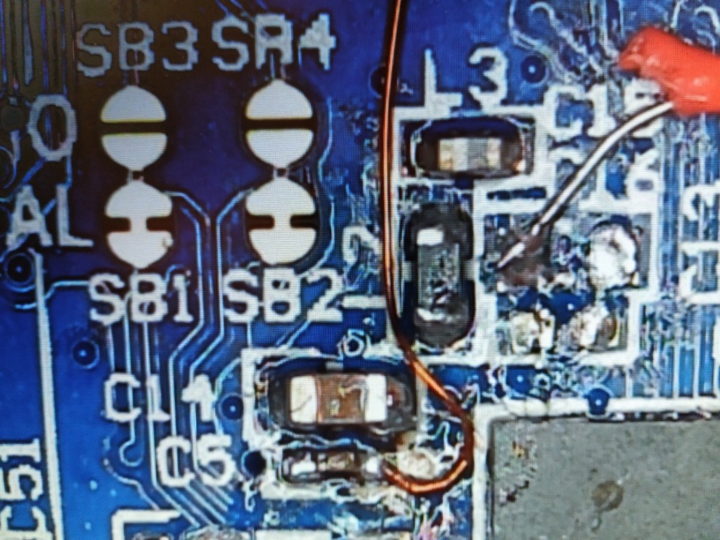
Under the binocular to solder wires on DEC1 (CPU Power) and DEC4 (System Power).
Note: I re-soldered a 100nF capacitor at C5 location to have more “stability” of the CPU power during boot-up. This is not really necessary but it can help in case of unexpected CPU crashes.
I connect the two wires to SMA connectors and I use a GND point as a common ground:
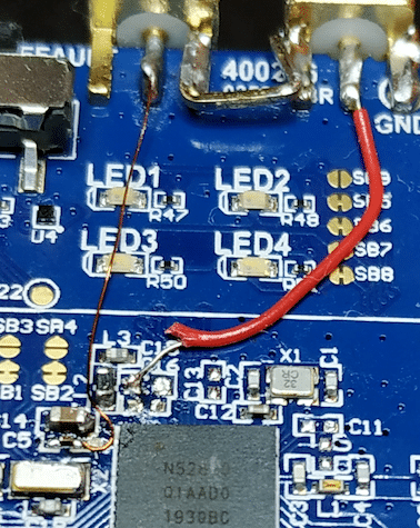
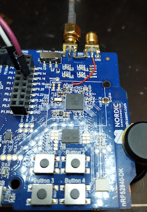
A micro-USB cable is used to power the entire board. USB to Serial Cable is connected to display UART message from the application (115200, 8N1).
6.5 Scope config
The oscilloscope is connected to the target:
- CHANNEL1 (CH1) = TxD (pin P0.06)
- CHANNEL2 (CH2) = Power consumption of the chip through DEC1
- CHANNEL3 (CH3) = Pulse command for the glitch
- CHANNEL4 (CH4) = Power consumption of the chip through DEC4 (Scope Trigger)
7. The results
7.1 Black-Box Reverse
The goal is to identify a particular pattern into the power consumption, which could validated my previous assumption.
For that purpose, the CPU power consumption (CH2) on DEC1 and System power Consumption (CH4) on DEC4 are both monitored.
First, the Flash Memory Activity is clearly distinguishable (at the trigger T mark) and corresponds to successive read operations from Flash:
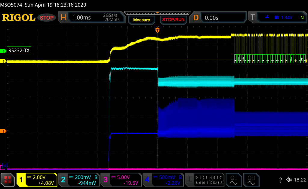
Scope Screenshot monitoring the nRF52840 Power-Up. CH1= UART, CH2 = CPU power, CH3 = glitch command (not activated) and CH4= System Power.
On the next screenshot, the Arm CPU starts its execution (at 19us after the trigger mark). It is distinguishable on CH2 (CPU power consumption):
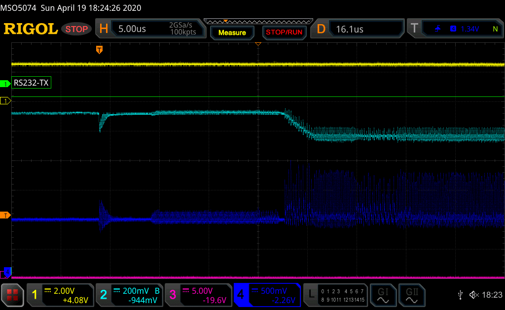
CPU starting its execution. CH1= UART, CH2 = CPU power, CH3 = glitch command (not activated) and CH4= System Power.
Then, I decide to focus my analysis to find the NVMC activity, by comparing the two power signals DEC4 and DEC1:
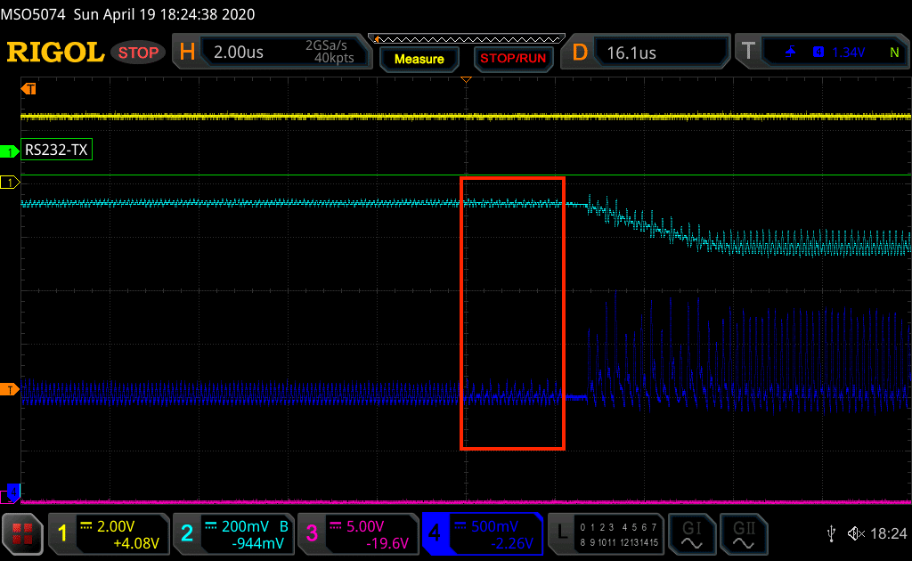
NVMC initialisation . CH1= UART, CH2 = CPU power, CH3 = glitch command (not activated) and CH4= System Power.
I am quite confident this pattern (red frame) corresponds to the memory controller (NVMC) transferring the UICR values to the core (or to the AHB-AP block directly), to configure the Debug Ports (AHB-AP, CTRL-AP) and set the APPROTECT to finally disable the debug interface.
7.2 Bypass the APPROTECT on nRF52840
A python script is in charge to arm the scope, set the different glitch parameters and reset the board.
A glitch campaign is started, producing very short pulse on the DEC1 power line to target specifically the previous identified pattern.
The next scope screenshot shows a successful glitch attempt:
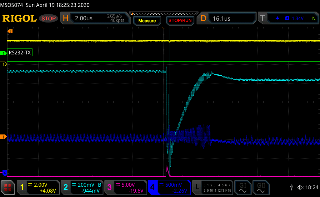
NVMC initialisation . CH1= UART, CH2 = CPU power, CH3 = glitter command (not activated) and CH4= System Power.
Note how the power consumption of the System is modified after the glitch. This is the result you want to obtain.
After each glitch attempt, the following OpenOcd command is then played by the script, in order to dump the entire Flash memory (this will happen only in case of successful connection to the AHB-AP Debug interface):
$ openocd -s /usr/local/share/openocd/scripts -f ./interface/jlink.cfg -c "transport select swd" -f ./target/nrf52.cfg -c "init;dump_image nrf52_dumped.bin 0x0 0x100000"
The AHB-AP Debug Port is successfully unlocked by the glitch effect. The external debugger can now connect to the nRF52840 CPU (cortex-M4F) to dump the Flash memory:
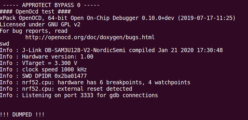
Debugger connected to the target nRF52840 despite the APPROTECT activated.
An Arm GDB session is then attached. Even if the APPROTECT value shows the nRF52840 is protected (0xFFFFFF00), it is now possible to debug the target, for example by reading the Firmware at 0x00000000:
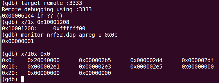
GDB session connected to the target nRF52840 despite APPROTECT activated.
7.3 PoC: Full Debug Capabilities
You probably guess it's also possible to fully control the device (because the debug interface is reactivated).
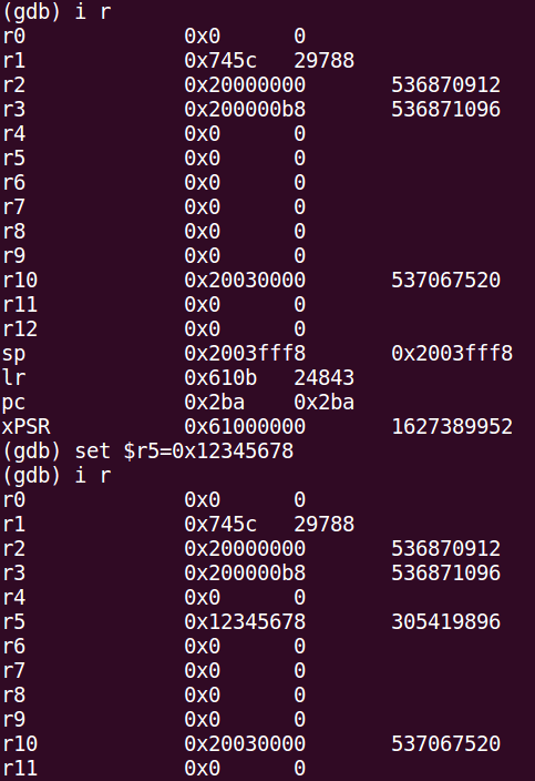
During my experiment, the CPU is stuck in endless loop at 0x61C4 after the glitch. So, the screen below shows how the Program Counter (PC) is set to execute the first instruction (at 0x2b4) then step-in into the code as Proof-of-Concept:
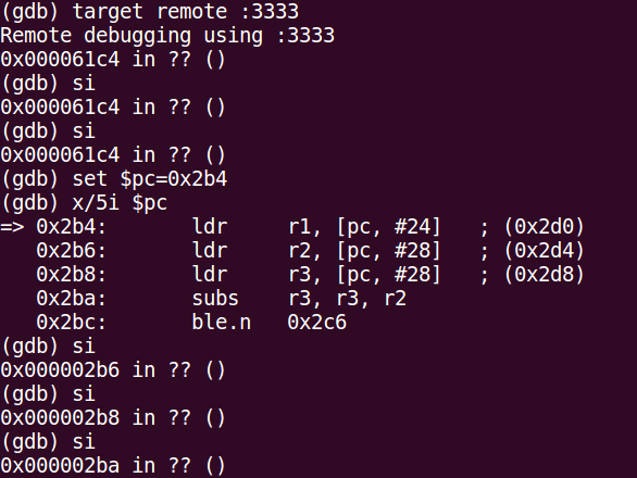
Code execution on a protected nRF52840.
R/W Access to Registers is below (SRAM and Flash R/W operations are available too, trust me):
Full Debug Capabilities, making future reverse easier :)
This PoC proves control of Flow Execution and R/W access to memories and registers.
7.4 Access to the FICR
Factory information configuration registers (FICR) are pre-programmed in factory and cannot be erased by the user. These registers contain chip-specific information (device id, keys, device address...) and are located at 0x10000000:
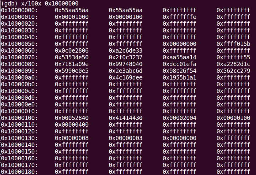
Factory Info Configuration Registers dumped
7.5 Adding persistence to the Exploit
Finally, the goal is to reactivate permanently the full debug capabilities on the device under test. The scenario is the following:
- Dump the Flash memory at 0x00000000
- Dump the UICR at 0x10001000
- Erase the device_: nrfjprog -f NRF52 --recover_
- Reflash the nRF52 again to write the Flash memory content and the UICR (with a proper patch of the APPROTECT value set to 0xFFFFFFFF of course).
After that, Debug over the SWD interface is enabled and the glitching attack is not necessary.
Enjoy.
8. Come on LR..."hacking dev-kit is easy"
Some people can say : "Always easy to hack dev-kit..."
OK, you're right and I am agree :)
To demonstrate how easy it is to apply this exploit, the attack has been reproduced on a real product, my Logitech Pro G Mouse.

RIP my little girl...
This will be the part 2 of this investigation of the nRF52 SoCs. I will demonstrate how this vulnerability is currently impacting ALL the nRF52 SoCs, from nRF52810 to nRF52840.
9. Conclusion
The Access Port Protection APPROTECT is the most recent security feature designed by NordicSemiconductor to protect against Firmware Readout and Reverse-Engineering. This APPROTECT feature is therefore present into the entire nRF52 SoCs Family.
In this blogpost, a low-cost fault attack has been successfully achieved on nRF52840. It allows an attacker having physical access to bypass the APPROTECT to reactivate the SWD debug interface permanently (R/W access to memories and registers, control CPU code execution, dump the Flash memory, FICR and UICR...)
Due to its low-complexity, this attack on the nRF52840 can be reproduced on the field easily. I have no doubt any motivated proficient hacker could reproduce this attack in less than one day and with less than 500$ equipment.
The vulnerability resides in Silicon. There is no way to patch without HW revision. This is impacting a tremendous number of products based on nRF52 platforms.
10. Timeline Disclosure
17/04/2020: Nordic PSIRT contacts LimitedResults.
22/04/2020: Nordic PSIRT proposes to purchase the full report for a rock-bottom price.
22/04/2020: LimitedResults says "No, sorry" (and stays polite).
28/04/2020: LimitedResults proposes to work with Nordic on a responsible disclosure based on CVE process.
29/04/2020: Nordic PSIRT is positive but does not provide any guarantees.
29/04/2020: LR asks for proper guarantees.
08/06/2020: After one month of silence and several follow-ups without any response from Nordic PSIRT, Nordic PSIRT declines to work with LimitedResults on a responsible disclosure.
10/06/2020: Posted.
[edited] 12/06/2020: Nordic have emailed all their customers with the following information notice here.